

How To Write Shift Register Without Shiftout Code For Arduino
Using a Shift Register to Control a Agglomeration of LEDs
Shift registers are very useful tools; using a few pins connected to a shift register, we tin can increment the number of output data pins that are bachelor to usa.
In this experiment, we'll be using a shift register to command eight LEDs, but we'll simply be using three pins from the ATmega.
Shift Register
A shift register is an external integrated circuit (IC) that can be used to expand the number of output pins bachelor to u.s.a.. Essentially they permit you turn serial input from a single pin (one fleck after the other) into multiple parallel output signals (all at once on separate lines).
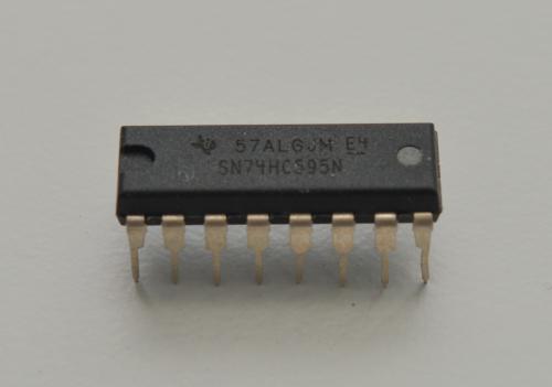
The shift register used in your kit is the popular 74HC595. It has viii output lines which allows you to dispense and use bytes for output in your code.
Overview
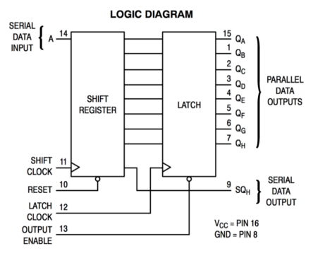
So how does this work? The IC is fabricated upward of two registers, units of retentivity that can hold up several binary values in order (8 for the IC in your kit). They are:
- The shift register, which holds 8 values before they are written to the output pins. Values tin can be "shifted" through this register from one position to the next, starting at position "A" to position "H".
- The storage register, which takes values from the shift register and sends them to the data output lines, labelled
QAtoQH. For instance, a logical1in position "C" of the storage annals would create a High signal onQC.
In that location are three pins on the IC that we use to control it with the Omega. Two of these pins are clocks: special inputs that trigger the IC to practise something when they receive a betoken that changes from LOW to Loftier (besides known equally a pulse or a rising edge).
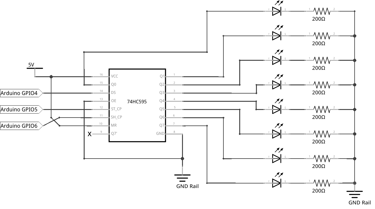
| Pin | Proper name | Purpose |
|---|---|---|
| SER | Serial data pin | This is the serial data input line. When we pulse the serial clock (SRCLK), the signal on this line is stored in the 1st position ("A") of the shift register. |
| SRCLK | Series clock | When pulsed, shifts each value in the shift register forwards by one position, and so loads the value from the SER pivot into position "A". Notation that this does not change the signals on the output lines until you pulse the annals clock (RCLK). |
| RCLK | Register clock, or "latch pin" | When pulsed, updates the storage register with new values from the shift register, sending a new set of signals to the 8 output pins. This happens and so rapidly that they all seem to change simultaneously! |
Chip Order
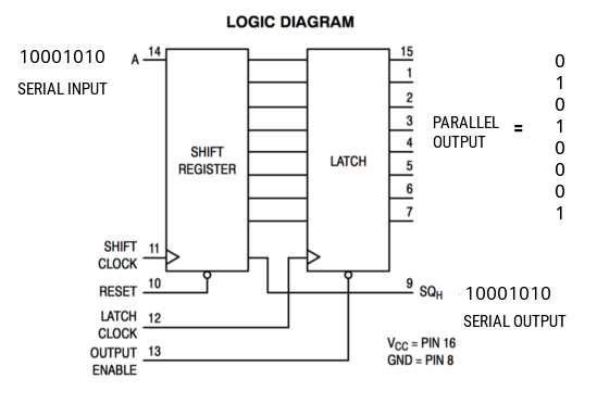
Keep in listen that the showtime value you send the shift annals will be shifted towards the final output pin as you send it more information.
Let's say we want to send the post-obit bits: 10101010. Intuitively, information technology seems easiest to send each bit in the number from left to right as if it were a cord. In Python, this would wait something like:
However, sending information technology this fashion means that after nosotros've sent all 8, the 1st bit would actually be shifted all the style to the last output (QH), the 2nd bit would exist shifted to the 2nd-to-last output (QG), and so on until everything is reversed! This way of shifting values out is known every bit nearly-significant bit (MSB) first. If we used this method in our shift annals class, we would take to wire everything upwards backwards, and this could brand it confusing to get together or debug circuits.
We tin can get around this consequence by sending the rightmost, or least significant scrap (LSB), first. Nosotros tin modify the to a higher place code into something like this:
Pinout Diagram
The pinout diagram for the 74HC595 is shown below:
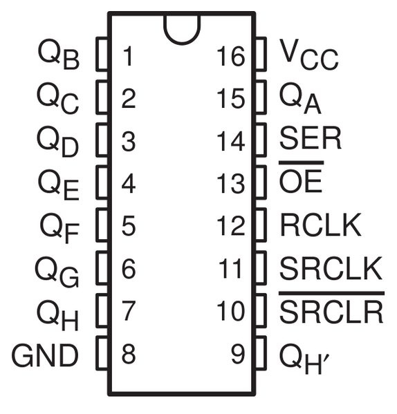
On the right side of the chip, you can see the iii control pins described above, equally well as the first output (QA). On the left side, yous can see the other 7 outputs (QB - QH).
Decision-making a Shift Annals
So how can this let u.s. control multiple outputs with one data pin? Well, permit'south say nosotros have 8 LEDs hooked upwardly to the data lines, and we want to turn on the second, 4th, and the 8th LEDs like and then:
| LED | Data Line | Desired Value |
|---|---|---|
| 1 | QA | LOW |
| two | QB | HIGH |
| 3 | QC | Low |
| 4 | QD | Loftier |
| 5 | QE | LOW |
| 6 | QF | Depression |
| 7 | QG | Depression |
| 8 | QH | Loftier |
Starting time, we'll clear out the register so all LEDs are off past writing eight 0's to the shift register, then pulsing the latch pivot to write the outputs to the information lines. This is washed by setting and holding SER LOW, then pulsing SRCLK 8 times, and so pulsing RCLK once.
So, using the LSB method, we will reverse the bytestring to get 10001010. For each of these values:
- Gear up SER to the specified value (HIGH or LOW).
- Pulse SRCLK from LOW to HIGH to shift the value of SER into the shift register.
We echo the 2 steps above (for instance, by using a loop) until all 8 values have been shifted in. Then pulse the RCLK pivot to write these values to the storage register and data lines, which turns on the LEDs!
In this way, we can command up to 8 dissimilar outputs with simply 3 GPIOs. This is an incredibly powerful technique that you can use to work with many components at once.
Here'due south the diagram from before to summarize what we've just described.
Daisy-Chaining
Shift registers can also be continued in serial to each other to extend the number of data lines that can be controlled at once. We can do this by using the QH' pin, which is connected inside the shift annals to the terminal output QH.
Merely connect the SER pin of one shift annals to the QH' pivot on another, and connect their SRCLK and RCLK pins together. That way, when you pulse SRCLK, the 2nd fleck will read from the concluding output of the 1st, and when you pulse RCLK, both chips volition update their output lines. This is great because this does non require any boosted GPIOs from the Omega!
Y'all've now just created a 16-bit shift annals, and you can extend the concatenation further past adding more than chips in the same mode equally above. This is known as daisy-chaining.
Detailed Specifications
if you're curious about the clock cycle timings or other information about the IC, you tin refer to the datasheet for the SN74HC595 shift annals. The clock bike timing diagram tin be found on folio 8.
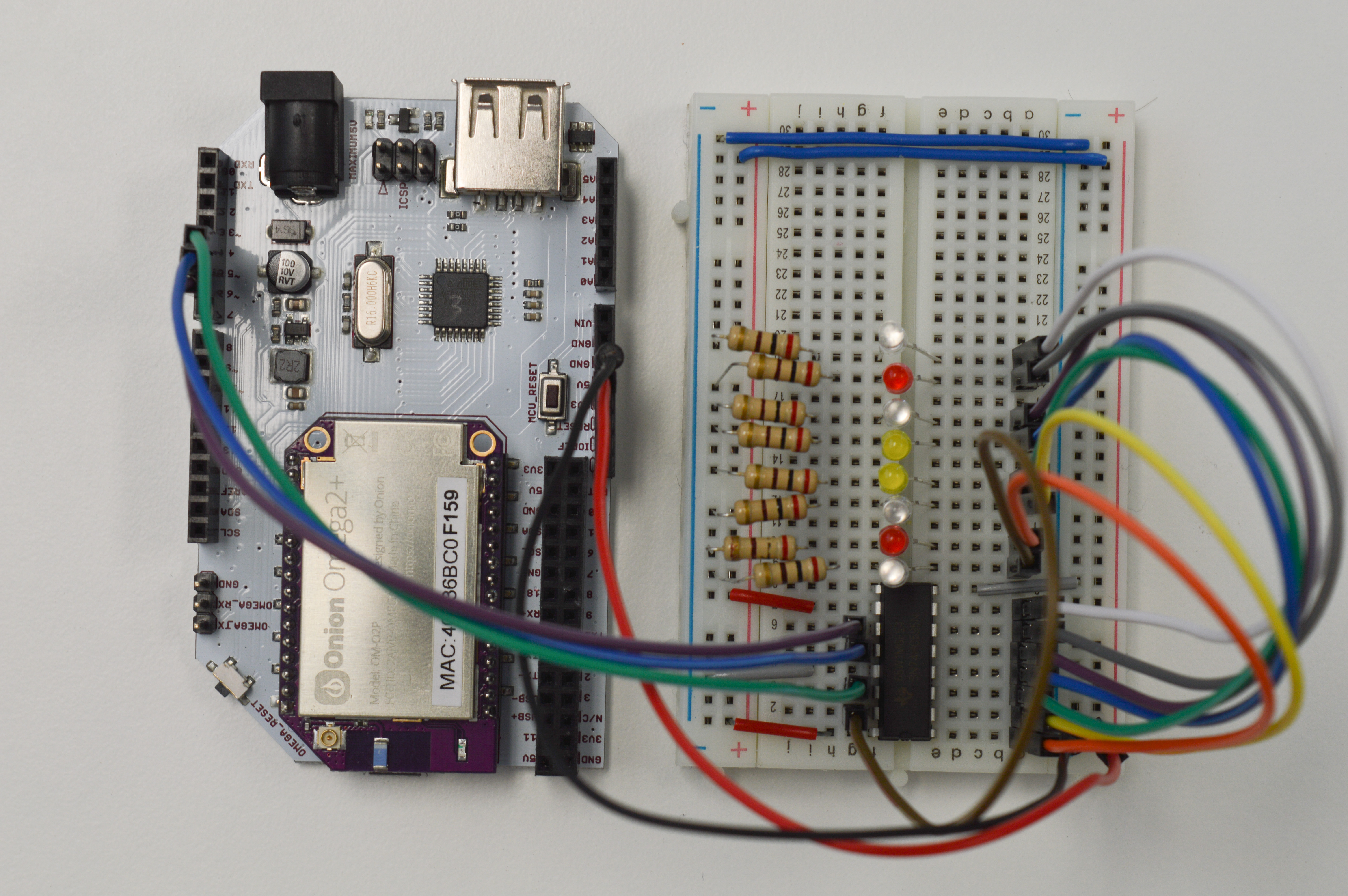
Building the Circuit
For this experiment, we will send a 8 $.25 (a byte) serially from the ATmega to the shift register. When the latch pin of the shift register is set Depression, the shift register will use the stored 8 $.25 to set its 8 output pins accordingly. We will attach one LED to each of the 8 output pins and make them light upward like Knight Rider's KITT. By the ability of the shift register, nosotros can exercise this using only three ATmega pins!
This is the diagram of the excursion we'll be building:
What You'll Need
Ready the following components from your kit:
- Omega plugged into Arduino Dock
- USB Micro-B cable for power
- Breadboard
- Jumper wires
- 8x 200Ω Resistor
- 8x LED color of your choice!
- 1x 74HC595 Shift register
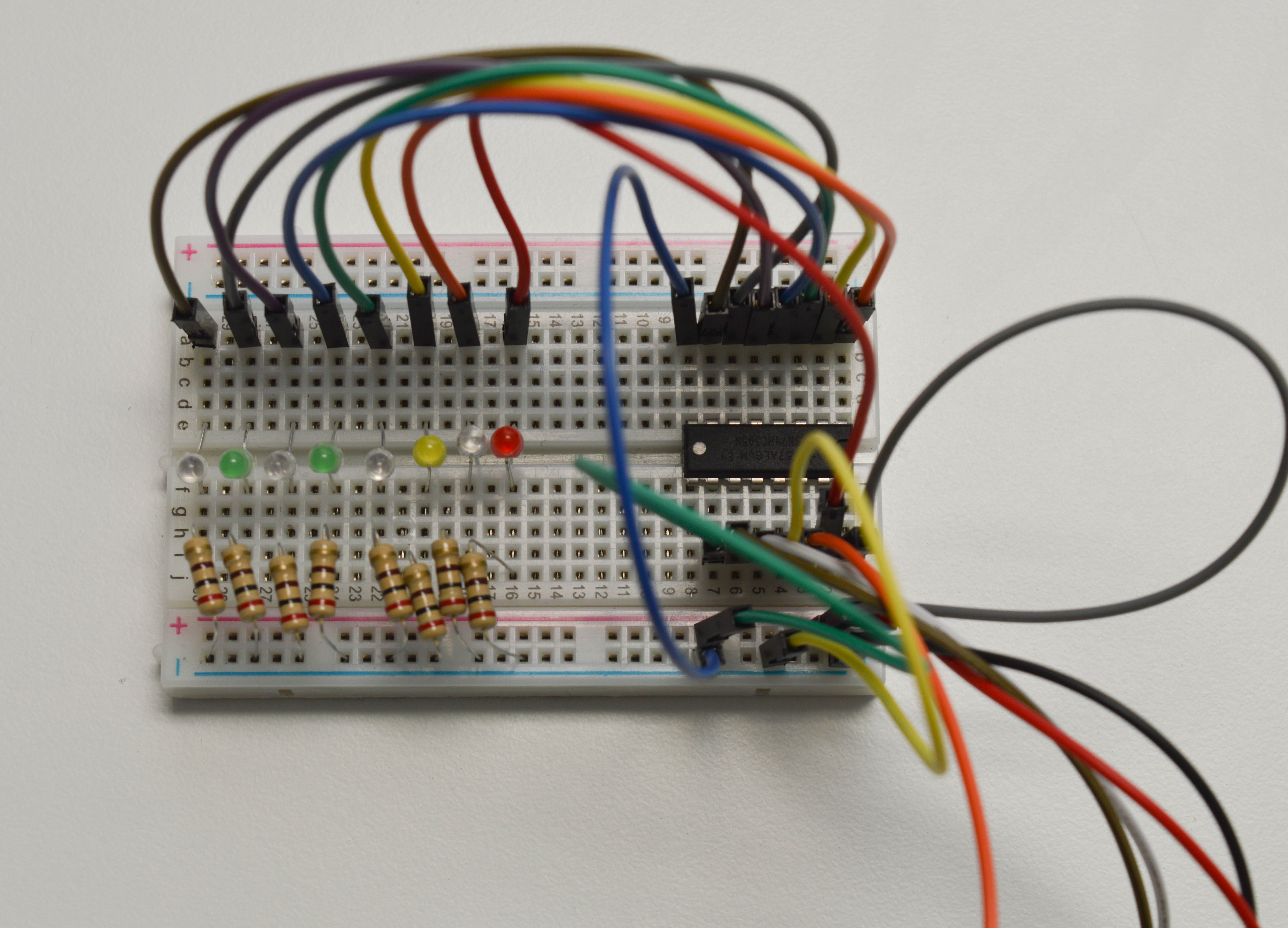
Hooking up the Components
The IC should be plugged in across the channel of your breadboard (the slot running down the center separating the abcde columns from the fghij columns). If you don't do this you will curt out the pins across your IC. You may need to bend the pins just a chip in society to get it to fit.
Lets take a look at how the xvi pins of the 74HC595 shift register scrap are defined. Nosotros'll exist referring to each pin by the numbers provided in the diagram above. When plugged in with the letters being right-side up, the bottow row of pins are pivot 1 to eight going from left to right. The pinnacle row of pins are pivot nine to sixteen going from right to left.
Annotation: Your IC volition have a semi-circle indentation that indicates "upwardly". Make sure that you plug information technology in properly so yous know which pins are where.
Here'south the steps to become there:
- Connecting your shift register to the breadboard
- Start past plugging in your shift register across the channel so that the each pivot has its own row.
- Connect the supply voltage pin (
Vcc) and the master reset pin (MR) on the IC to theVccrails on the breadboard - Connect the
GNDpin and output enable pin (OE) to theGNDrail on the breadboard
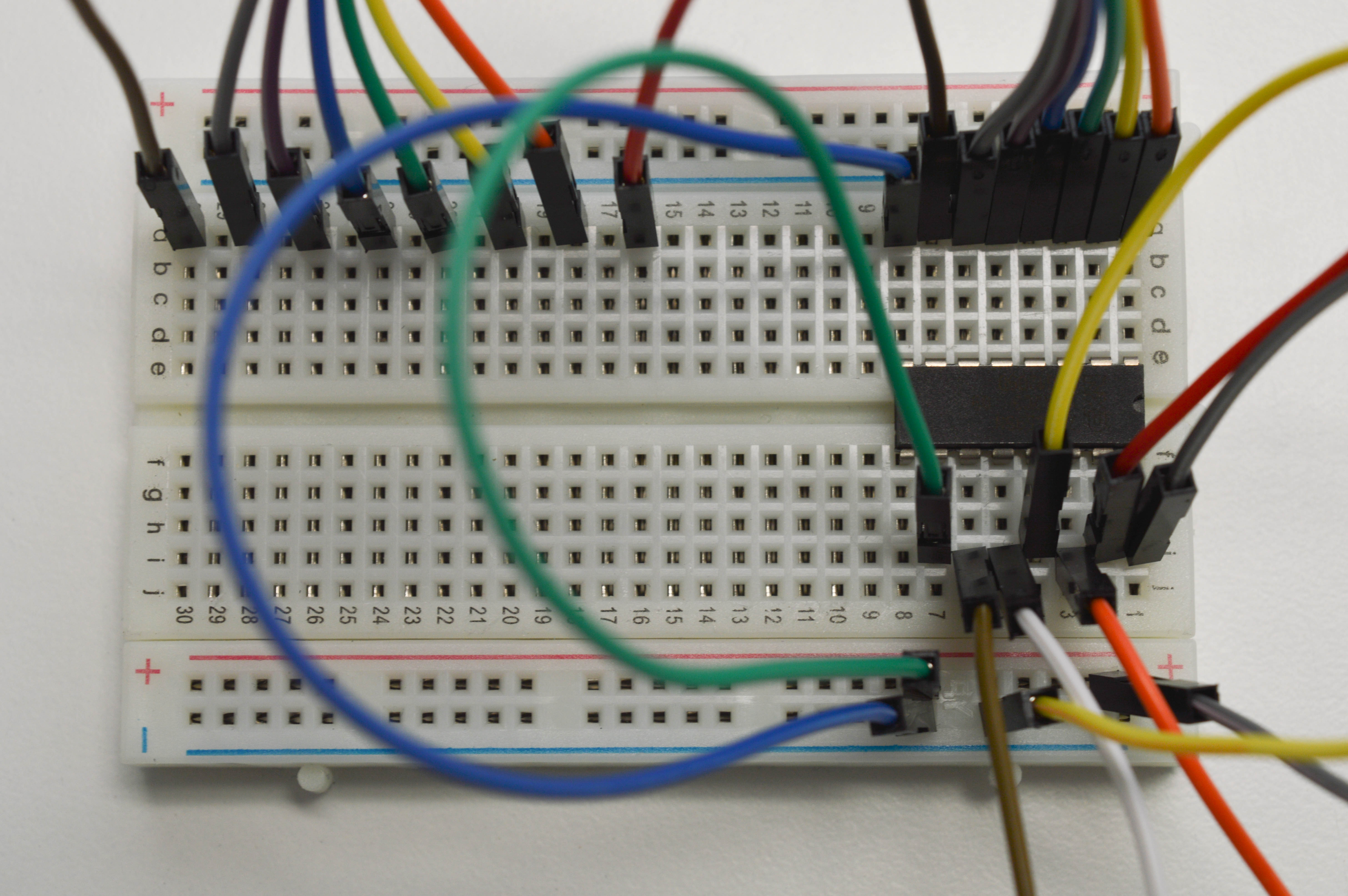
The jumpers at the top will exist wired to the LEDs eventually.
- Connecting your LEDs
- Connect the anodes of the eight LED each to one of the eight output pins of the 74HC595 - pin
fifteenand pinaneto7, corresponding toQ0toQ7. Place the LEDs left to correct in the following pivot social club:Q0,Q1,Q2,Q3,Q4,Q5,Q6,Q7.
- Connect the anodes of the eight LED each to one of the eight output pins of the 74HC595 - pin
- Attach eight 100Ω electric current limiting resistors from cathodes of the LEDs to the
GNDrail on the breadboard.
- Connecting your Arduino Dock
- Connect the
GNDpin on the Dock to theGNDrail on the breadboard. - Connect Arduino Dock digital pin 4 to
DSon the shift register - this is where our input is sent. - Connect Arduino Dock digital pin 5 to
STCPon the shift annals. - Connect Arduino Dock digital pivot half-dozen to
SHCPon the shift annals. - Connect the
Vccrail to a5Vpivot on the Arduino Dock
Writing the Code
#ascertain NUM_LEDS 8 // duration to pause int delayTime = 100; // the pivot continued to the latch pin, RCLK (pivot 12 of the shift register) // setting the latch Depression will send the viii $.25 in storage to the output pins int latchPin = 5; // the pin connected to the clock pin, SRCLK (pivot 11 of the shift annals) int clockPin = half dozen; // the pin connected to the series data pivot, SER (pivot 14 of the shift annals) int dataPin = iv; // This code runs once when the program starts, and no more void setup() { // initialize all the pins continued to the shift register every bit outputs pinMode(latchPin, OUTPUT); pinMode(dataPin, OUTPUT); pinMode(clockPin, OUTPUT); } // office which sends the stored byte to the output pins by setting the latch pin LOW void updateShiftRegister(byte storageByte) { // prepare the latch pin Low digitalWrite(latchPin, Depression); // transport the storage byte to the shift register with the LSB first // since the latch is LOW, fix the viii output pins based on the stored 8 bits and in turn calorie-free the correct LED shiftOut(dataPin, clockPin, LSBFIRST, storageByte); // set the latch pivot Loftier again digitalWrite(latchPin, HIGH); } // The code in here will run continuously until we turn off the Arduino Dock void loop() { // the byte (8 bits) to be stored in the shift register // initialize to 00000001, representing the beginning LED on byte storageByte = 0x01; // create the effect of having the low-cal travel to the left for (int i = 0; i < NUM_LEDS-1; i++) { // ship the viii bits to the shift register and prepare latch LOW updateShiftRegister(storageByte); // bitwise shift to the left by 1 chip // the MSB will disappear and a 0 will be shifted in for the LSB // ex. 10000001 to 00000010 storageByte = storageByte << 1; // wait earlier moving on to the next LED to enhance the animation delay(delayTime); } // create the issue of having the lite travel in the contrary management for (int i = 0; i < NUM_LEDS-1; i++) { // ship the 8 bits to the shift register and set latch LOW updateShiftRegister(storageByte); // bitwise shift to the right past ane bit // the LSB will disappear and a 0 will exist shifted in for the MSB // i.east. 10000000 to 01000000 storageByte = storageByte >> one; // expect before moving on to the adjacent LED to enhance the blitheness filibuster(delayTime); } } What to Expect
The eight LEDs volition light up like KITT from Knight Rider. The first LEDs will plow on, then the next will plow on and the previous 1 will plow off. This will echo for all the LEDs in a loop from left to right and and then from right to left. Only i LED should be lit up at a time.
It should expect a little like this:
See, simply like KITT:

A Closer Look at the Code
We are only using three Arduino Dock pins to command viii LEDs past taking advantage of the shift annals. Lets begin by declaring the three pin variables (latchPin, clockPin and dataPin) and initializing the 3 pins as output in setup().
Each time we desire to light up a unlike LED, we update the shift register to send the shift register new signals for each LED.
Updating the Shift Register
We control the shift register using a single office updateShiftRegister. The first thing information technology does is to set the latch pin low using a call to digitalWrite():
Then nosotros use a part that'southward included in the default Arduino libraries, shiftOut(), to send the byte:
This function does the following actions:
- Sets the SER pivot to either High or Low according to the bit of the byte you want to ship
- Sets the clock pivot High, so LOW to load the SER chip into the shift register
- Repeats the higher up two steps until all $.25 in the byte have been sent
The role takes an argument, bitOrder, which determines whether it sends the right-most (least significant) bit, or the left-most (well-nigh significant) flake first. Here we've decided to transport it least significant bit first (LSBFIRST) so that our wiring society can match the order of the shift register's outputs.
Once the byte has been sent, we set the latch pin HIGH to trigger the clock that updates the shift annals'due south outputs. This is done with another phone call to digitalWrite():
You lot'll observe we left in a slight delay earlier every update. This is because if we let it run as fast the CPU can go,it will be likewise fast for united states to see. Instead, the lights volition appear as if they were all on at the aforementioned time. The shift register tin accurately update at 100MHz - much faster than our eyes tin can perceive! In order to really encounter the outcome, we deadening it down by calculation the delay.

How To Write Shift Register Without Shiftout Code For Arduino,
Source: https://docs.onion.io/omega2-arduino-dock-starter-kit/arduino-kit-shift-register.html
Posted by: donofriohisidest.blogspot.com
0 Response to "How To Write Shift Register Without Shiftout Code For Arduino"
Post a Comment